HPA controller build

dstroy

Insanely Active Member
Not all of the power supplies are redundant. Just +24,12,5,3v3 bus voltages. Then +9 and +5v for the microcontrollers.

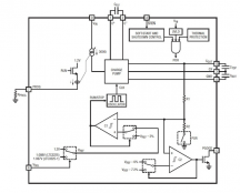
Two batteries, one main battery and an emergency lipo to charge supercaps. I'll build a chargepump to charge the caps from the battery.

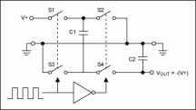
Something like this but with a bank instead of two caps, and +12vout.
Capture.PNG


I will have a better idea of what size and discharge rate of battery that I need when I determine the charging characteristics of the supercapacitors and output of the charge pump circuit.
 

ChiefRunningPhist

Drunk on Knowledge
Not all of the power supplies are redundant. Just +24,12,5,3v3 bus voltages. Then +9 and +5v for the microcontrollers.

Two batteries, one main battery and an emergency lipo to charge supercaps. I'll build a chargepump to charge the caps from the battery.

Something like this but with a bank instead of two caps, and +12vout.

View attachment 9244


I will have a better idea of what size and discharge rate of battery that I need when I determine the charging characteristics of the supercapacitors and output of the charge pump circuit.
I didn't know the EMI would be an issue, I thought at low wattages and correct spacing, that the PCB interference, let alone the WiFi interference would be negligible. But that shows my naivete I guess lol.

I'm working on power distribution as well but due to the PS being CC, Im only worying about regulating current and so won't have a bunch of inductors creating EMI to deal with, I'm still testing to see how the PS likes it.

I'm also working on a super cap charging and discharging regulator.

Haven't looked too much into the super cap portion of my cct but pretty sure Ill be relying on lm358s for PWM generation and comparator purposes in regulating the super cap.

What IC is that? Or is that just your charging cct layout? I can't find any SCCs rated for 24V. Is this why you're building your own charge pump?

I'm assuming you'll be following something basically like this for your custom charge pump design? Change caps and frequency and change max Vin and Vout?
A197Fig01.gif

Sorry for the 20 questions but I'm just curious and learning as I go. It seems you've got a good handle on things and I'm particularily intrigued by your custom charge pump.

EDIT:
I missed that you're using a battery to charge the super cap (power the charge pump), oops!
 
Last edited:

dstroy

Insanely Active Member
Probably this


I didn't know the EMI would be an issue, I thought at low wattages and correct spacing, that the PCB interference, let alone the WiFi interference would be negligible. But that shows my naivete I guess lol.

I'm working on power distribution as well but due to the PS being CC, Im only worying about regulating current and so won't have a bunch of inductors creating EMI to deal with, I'm still testing to see how the PS likes it.

I'm also working on a super cap charging and discharging regulator.

Haven't looked too much into the super cap portion of my cct but pretty sure Ill be relying on lm358s for PWM generation and comparator purposes in regulating the super cap.

What IC is that? Or is that just your charging cct layout? I can't find any SCCs rated for 24V. Is this why you're building your own charge pump?

I'm assuming you'll be following something basically like this for your custom charge pump design? Change caps and frequency and change max Vin and Vout?
View attachment 9257

Sorry for the 20 questions but I'm just curious and learning as I go. It seems you've got a good handle on things and I'm particularily intrigued by your custom charge pump.

EDIT:
I missed that you're using a battery to charge the super cap (power the charge pump), oops!
 

ChiefRunningPhist

Drunk on Knowledge
Probably this

And here's the actual charger

pretty scalable

I'll take a peek, sounds pretty nice
 

dstroy

Insanely Active Member
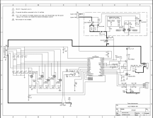
This is TI's reference design using the bq33100 frontend

9445

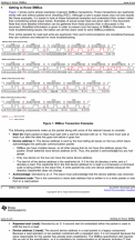
Could just put some level shifting on here to make it i2c compatible out of the box. The communication protocol is similar. I think the wire library works with it. Sometimes they have a weird start stop thing. I haven't read enough into making it compatible since I really just want something i2c and will use this if I can't find something more economical.
 

ChiefRunningPhist

Drunk on Knowledge
This is TI's reference design using the bq33100 frontend

View attachment 9445

Could just put some level shifting on here to make it i2c compatible out of the box. The communication protocol is similar. I think the wire library works with it. Sometimes they have a weird start stop thing. I haven't read enough into making it compatible since I really just want something i2c and will use this if I can't find something more economical.
I think if your clock is under 100khz that smbus and I2C can be interchangeable but I really don't know much about it.

Idk if I'm quite comprehending. At which TB is the cap bank? TB2, TB3, & TB4 are for sup cap connection? How many sup caps can it monitor? At first glance I thought p1-p5 were sensor inputs that controlled loads r14-r17, and r31, but after zooming out that seems incorrect.

It seems like Bq33100a just monitors the cap bank and that bq24640 is the actual charging IC.

Looks like I'll be doing some reading lol
 

dstroy

Insanely Active Member
I think if your clock is under 100khz that smbus and I2C can be interchangeable but I really don't know much about it.

Idk if I'm quite comprehending. At which TB is the cap bank? TB2, TB3, & TB4 are for sup cap connection? How many sup caps can it monitor? At first glance I thought p1-p5 were sensor inputs that controlled loads r14-r17, and r31, but after zooming out that seems incorrect.

It seems like Bq33100a just monitors the cap bank and that bq24640 is the actual charging IC.

Looks like I'll be doing some reading lol
5 caps in series for the advanced monitoring per cap.

tb2 is the cap, with 1n the gnd and 1p the first cap.

Correct, the bq33100 controls and monitors the charger, and the supercaps.
 

ChiefRunningPhist

Drunk on Knowledge
5 caps in series for the advanced monitoring per cap.

tb2 is the cap, with 1n the gnd and 1p the first cap.

Correct, the bq33100 controls and monitors the charger, and the supercaps.
So...

Screenshot_2019-06-08-19-09-53.png
Screenshot_2019-06-08-19-08-57.png

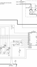
J1 is your data line hookup, TB4 is an auxiliary discharge output, pin23 on the monitor IC is driving the gate at Q6 between the cap bank and charging cct/main power rail, and pins 11 & 12 are driving gates at Q1 & Q2 which depending on sequence are regulating charging voltage? TS pin is a safety precaution for shutting down upon high temp?

Seems pretty nice if I'm comprehending.

Im not using an rpi in my sup cap charge/discharge cct, and so was going to build the charge/discharge cct with more or less passive components, (lm358s SSRs, and MOSFETs too) but having the capability to monitor the sup cap, especially if there's multiples like a bank setup, now seems pretty convenient & nice. I really haven't messed with rpi at all so I have been avoiding it, but perhaps I just need to embrace it lol

EDIT:
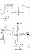
Didn't see D3 earlier, so TB4 is not an aux(?) but the actual discharge output? Can't figure how its discharge is being regulated then/now, now that it can't go back through charging cct to reach power rail, I don't see any FET in the dishage path? Is this only for charging and monitoring? Regulating discharge will be a different cct or IC?

EDIT: EDIT:
Lol, maybe LLEN pin is driving gate at Q8 to regulate discharge?
 
Last edited:

dstroy

Insanely Active Member
So...

View attachment 9459
View attachment 9460

J1 is your data line hookup, TB4 is an auxiliary discharge output, pin23 on the monitor IC is driving the gate at Q6 between the cap bank and charging cct/main power rail, and pins 11 & 12 are driving gates at Q1 & Q2 which depending on sequence are regulating charging voltage? TS pin is a safety precaution for shutting down upon high temp?

Seems pretty nice if I'm comprehending.

Im not using an rpi in my sup cap charge/discharge cct, and so was going to build the charge/discharge cct with more or less passive components, (lm358s SSRs, and MOSFETs too) but having the capability to monitor the sup cap, especially if there's multiples like a bank setup, now seems pretty convenient & nice. I really haven't messed with rpi at all so I have been avoiding it, but perhaps I just need to embrace it lol

EDIT:
Didn't see D3 earlier, so TB4 is not an aux(?) but the actual discharge output? Can't figure how its discharge is being regulated then/now, now that it can't go back through charging cct to reach power rail, I don't see any FET in the dishage path? Is this only for charging and monitoring? Regulating discharge will be a different cct or IC?

EDIT: EDIT:
Lol, maybe LLEN pin is driving gate at Q8 to regulate discharge?
The supercaps discharge if the line voltage droops or disappears, they can hold up the line.

Capout is the “supply”

Those transistors and resistors are for parasitic balancing and discharging. Right next to the cap input.

Do you see that sense resistor at the bottom?
 

dstroy

Insanely Active Member
The difference between active and passive components is that passive components can't control electrical current by means of another signal.

For example, a mosfet is an active component. You supply a signal to the gate and it conducts current across the source and drain.
 

ChiefRunningPhist

Drunk on Knowledge
The supercaps discharge if the line voltage droops or disappears, they can hold up the line.

Capout is the “supply”

Those transistors and resistors are for parasitic balancing and discharging. Right next to the cap input.

Do you see that sense resistor at the bottom?
Lol yep, that makes sense, I was assuming a current dump like when you short a cap, but its just X volts and if there's a YΩ load in between it will discharge at Zamps. You can tell how far I've gotten on my super cap portion

And ya capout is more precise than tb4 but I'm following.

And I think so, R18(?), The one 6&7 are measuring?
 

dstroy

Insanely Active Member
Lol yep, that makes sense, I was assuming a current dump like when you short a cap, but its just X volts and if there's a YΩ load in between it will discharge at Zamps. You can tell how far I've gotten on my super cap portion

And ya capout is more precise than tb4 but I'm following.

And I think so, R18(?), The one 6&7 are measuring?
R18 is a sense resistor.

R5 and R6 dictate the charge output.

R4 and R7 form a voltage divider which uses the shunt current from that zener to regulate the charge voltage. Passive feedback.
 

ChiefRunningPhist

Drunk on Knowledge
The difference between active and passive components is that passive components can't control electrical current by means of another signal.

For example, a mosfet is an active component. You supply a signal to the gate and it conducts current across the source and drain.
Sure, I understand active and passive, op amps mosfets and and ssr's are all active. I was more or less saying I wasn't using charging ICs, rather I was building my own, and without the added data transmission its less complicated and more manageable to create at my current electronics level aha
 

dstroy

Insanely Active Member
Sure, I understand active and passive, op amps mosfets and and ssr's are all active. I was more or less saying I wasn't using charging ICs, rather I was building my own, and without the added data transmission its less complicated and more manageable to create at my current electronics level aha
My current electronics design level isn't all that advanced. I'm learning as I go. I fixed things for a long time, and can follow a schematic. Usually other people make those schematics for me to read.
 

ChiefRunningPhist

Drunk on Knowledge
It all made sense when I realized the current dump wasn't happening lol before that i was really questioning my comprehension. They may as well be batteries and im not used to thinking of cap discharge times greater than ms because all I've mainly used them for is timing caps in pwm generation.

Is the data transmission dual? Like your rpi can command, ontop of the monitor can send to the rpi by itself?

EDIT:
I'm getting acquainted, had no idea, this stuff is sweet! Haha
Screenshot_2019-06-09-06-34-09.png
 
Last edited:
Top